
TSMC confirmed on April 12 that it is aggressively expanding its advanced packaging operations across Taiwan and the United States, moving beyond its already dominant CoWoS technology toward a next-generation format called CoPoS, and the scale of what they’re building is frankly hard to wrap your head around.
This is not a minor product update. This is a fundamental shift in how the most important chips on the planet get assembled, and it has massive implications for the future of artificial intelligence.
CoWoS was just the beginning
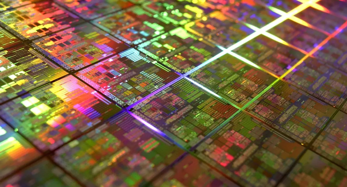
To understand why this matters, you need to understand what advanced packaging actually is. When people talk about chips getting more powerful, they usually think about transistors getting smaller. That’s true, but there’s a second, equally critical piece: how you physically connect multiple chips together inside a single package. That’s where TSMC has been quietly building one of its most important competitive advantages.
CoWoS, Chip on Wafer on Substrate, is the technology that makes NVIDIA’s H100 and B200 GPUs possible. It stacks the compute die alongside HBM memory modules on a silicon interposer, which is essentially a high-density communication layer that lets different chips talk to each other at extraordinary speeds. Without CoWoS, there are no AI accelerators as we know them. NVIDIA has effectively locked up the majority of TSMC’s CoWoS capacity through 2027, and demand isn’t slowing down.
According to US-based institutional investors cited in the April 12 CNA report, TSMC’s CoWoS-led advanced packaging capacity is expected to grow from 1.3 million wafers this year to 2 million wafers by 2027. That alone would be a remarkable expansion. But TSMC isn’t stopping there.
The problem with CoWoS is the shape of the wafer itself. Silicon wafers are round, which means significant surface area gets wasted around the edges when you’re packaging increasingly large AI chips. CoPoS, Chip on Panel on Substrate, solves this by switching to large rectangular panels instead of circular wafers, dramatically increasing how many chips you can process at once while reducing cost per unit. Institutional investors estimate that TSMC’s advanced packaging capex, covering CoWoS, CoPoS, and SoIC combined, will grow at a compound annual rate of 24% from 2025 to 2027.
That number tells you everything about where TSMC sees the future of this industry heading.
Taiwan builds it first, Arizona follows
TSMC already operates five advanced packaging facilities in Taiwan, spread across Hsinchu, Tainan, Longtan, Taichung, and Zhunan. But the real centerpiece of the Taiwan strategy is the new AP7 facility in Chiayi, which will host CoPoS, SoIC, and WMCM packaging technologies across a site spanning 15,000 square meters planned across eight phases. TSMC has said Chiayi will become its largest advanced packaging hub. The first CoPoS pilot line is targeted for 2026, with full mass production at Chiayi expected between late 2028 and 2029.
At the same time, TSMC is making a move that would have seemed almost unthinkable just a few years ago: building advanced packaging capacity inside the United States. Right now, every chip that comes out of TSMC’s advanced fabrication plant in Phoenix, Arizona gets shipped back to Taiwan for packaging. Every single one. That dependency is about to end. TSMC is investing $165 billion in Arizona, building up to 12 facilities including two dedicated advanced packaging fabs.
AP1 is expected to reach mass production by 2028 focusing on SoIC and CoW technologies, while AP2 will be built specifically around CoPoS. For the first time ever, the US will have a genuine end-to-end semiconductor manufacturing operation on its own soil.
The April 12 CNA report makes clear that this expansion is driven by TSMC’s biggest American clients: NVIDIA and AMD continue showing relentless demand for CoWoS, Apple’s high-end processors depend on TSMC’s InFO technology, and AMD is also one of TSMC’s top SoIC customers. These companies need supply chain certainty, and TSMC is building it for them, on two continents simultaneously.
What this really means for AI
Here’s the opinion part, and I’ll be direct about it: advanced packaging is becoming the single most important bottleneck in the entire AI industry, and not enough people are talking about it that way.
Everyone obsesses over process nodes, 3nm, 2nm, 1.6nm, but the real constraint on AI progress right now isn’t transistor density. It’s the ability to physically assemble chips fast enough to meet demand. As AI chips grow larger and more complex, the round 300mm silicon wafer becomes an increasingly inefficient medium for packaging them. CoPoS is the industry’s answer to that problem, and TSMC is the only company with the scale, the technology, and the customer base to actually pull it off at the speed AI demands.
The Arizona expansion adds another layer to this story. Building advanced packaging in the US isn’t just about politics or CHIPS Act subsidies, it’s about giving the global AI supply chain a second lifeline. The entire AI boom currently runs through a very small island in the middle of a geopolitically sensitive strait. Any serious disruption there doesn’t just hurt one company, it halts the AI industry worldwide. TSMC’s dual-location strategy is the most serious attempt yet to address that vulnerability.
Advanced packaging already represented roughly 8% of TSMC’s total revenue in 2025 and is expected to exceed 10% in 2026, with management projecting this segment to grow faster than the rest of the company in the coming years. That’s not a side business anymore. That’s a growth engine, and it’s one that will only accelerate as AI models get bigger, chips get more complex, and the demand for heterogeneous integration keeps climbing.
The transistor wars are far from over, but the packaging wars have already begun, and TSMC just showed everyone exactly how serious it is about winning both.
What do you think about TSMC’s bet on dual-continent packaging, smart long-term strategy or are there risks you’d be worried about? Leave your take in the comments!